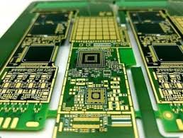
Designing and Fabricating HDI PCBs
High-Density Interconnect (HDI) PCB technology allows PCB designers to increase the amount of components and routing channels on a board. This increases functionality, reduces signal interference, and helps meet power and space requirements. However, designing and fabricating HDI PCBs requires precise manufacturing processes to produce the small features necessary for high-speed circuitry. These techniques include laser drilling and sequential lamination.
As the demand for more powerful and smaller electronic devices grows, so does the need to pack more components into a PCB. HDI technology allows PCB manufacturers to use more components, finer pitch, and advanced materials in a smaller area. HDI PCBs are also ideal for high-speed communications because they can transmit data more efficiently and minimize signal crossing delays.
PCBs are made by etching copper layers, separating them with partially cured laminates, and stacking them like a book. The laminates are then pressed and heated enough to liquify the prepreg used to hold the layers together. These liquified layers are then fused together to create the hdi pcb. To produce a board with blind and buried vias, the layers must undergo several numbers of sequential laminations. The process is more expensive than a traditional multilayer PCB, but it can offer the benefits of increased component and routing density.
Challenges in Designing and Fabricating HDI PCBs
One of the biggest challenges in designing and fabricating HDI PCBs is ensuring proper thermal management. Because the components and traces are packed more closely, they must dissipate heat quickly to avoid overheating and potential system failures. However, thin dielectric materials often have poor thermal conductivity, making it difficult to transfer heat away from the components and traces.
To compensate for this, PCB designers must reduce the thickness of traces and use smaller spaces to fit more components. This requires that they utilize DRC settings in advanced design tools and implement proper layout strategies. Additionally, it’s important to choose a reputable manufacturer that offers HDI services and stays informed of material advancements.
Another challenge is determining how to connect the various layers of an HDI PCB. Since the mechanical drill cannot produce holes smaller than 6 mils, a more precise via formation process is needed to place microvias between layers. The most common method is through-holes, but other techniques can be used as well, such as via-in-pad technology.
Other challenges include identifying the right PCB supplier for your project and establishing a budget that accommodates the extra costs of using HDI technologies. It’s important to work with a dependable partner who can provide quick turnaround and excellent customer service. Additionally, you should try to plan your orders in advance to save money and minimize costly rush charges. Moreover, you should always select a PCB supplier that can provide high-quality products for the best value. This will help to keep your PCB production costs low while maintaining a fast time-to-market.


Recent Comments